Basic Principles of Hyperspectral Imaging
Hyperspectral imaging technology has imaging and spectral function, in the detection target two-dimensional space at the same time, for each spatial position of spectral information, so as to realize the four dimensional space- (4D) material composition analysis, truly realize the physical world component digital, give equipment "critical", let the terminal to better understand the world.

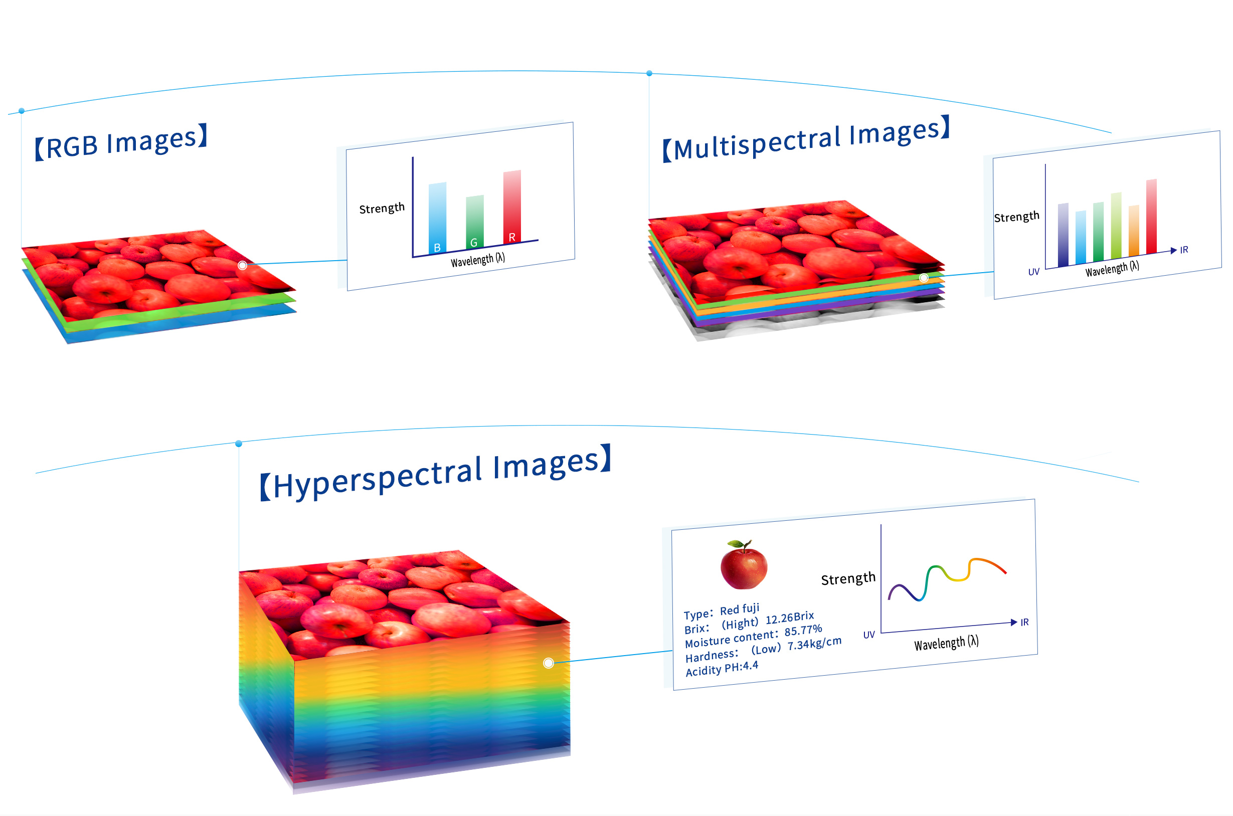
MEMS-Hyperspectral imaging sensor
Hypernano is the lead in mass production of the world's first movable mirror process hyperspectral imaging MEMS-FPI chip, which has the advantages of low power consumption, wide spectrum continuous tunable, high spatial resolution, fast speed (millisecond).

Hypernano have rich MEMS process development and MEMS standardized production process experience, master etching, coating, suspended, reflection and sealing cavity processing technology, can realize bulk process, surface process and bonding process and other different structure of FPI chip design and manufacturing, is a handful of domestic MEMS whole process production technology reserves of science and technology enterprises.
  • The earliest mass production, industrial landing
  • Miniaturization
  • Stepless tunable
  • Standardized mass production
  • Full spectral coverage
  • Real-time online
Technological superiority
Through years of continuous technological innovation, Hypernano made a breakthrough of the special technilogy of hyperspectral imaging chip, mastered core technology of full chain hyperspectral imaging , achieved the application of the hyperspectral imaging MEMS sensor, miniature module, camera and other core components, to intelligent home, industrial testing, environmental detection scenarios etc, booster physical world component digital process, enable industry intelligent upgrade.
Miniaturization
MEMS-Hyperspectral sensor have a volume reduction of over 1000 times compared to traditional spectral imaging devices and extremely low power consumption
Flexible and tunable
Wide spectrum continuously adjustable, imaging freely selectable
Applications
Empowering multiple industry sectors, promoting industrial intelligence and digital upgrading
Large field of view
Large field of view angle, wide field of view
Hardware
World's leader in hyperspectral MEMS technology, advanced hyperspectral modules, hyperspectral cameras, etc.
Real-time online
High spatial resolution and millisecond level response speed
Hyperspectral + AI algorithm
Hypernano's Hyperspectral data is combined with AI object detection algorithms for imaging images, with programmable wavelength selection for one-stop analysis of composition and other related issues; combined with machine learning and deep learning, it can reduce the demand for training data volume of the analysis system, and realise the prediction of large samples from small samples. In addition, HISP Nano hyperspectral data has high accuracy, is applicable to a wide range of scenarios, and has stable result output. Translated with www.DeepL.com/Translator (free version)

  • 13.5
    Brix
    Brix
  • 4.08
    Acidity
  • 8.13
    kg/c㎡
    Hardness
  • 83.8%
    Moisture content
Technical strength
  • ToP
    The world's top MEMS experts
    have many overseas high-level talents in Shenzhen
  • 70 %
    The core team of master and doctoral talents account for 70%+
  • 20 +
    Twenty years of experience in MEMS process development and manufacturing
  • 90 +
    Applied for 88 domestic and foreign patents ;
    42 authorized, 5 PCT patents